2. Materials and Methods
This section presents the structural, optical, and electrical properties of ZnSe thin films, followed by the electrical model used for the CIGS solar cell. The fundamental photovoltaic equations are introduced, and the numerical simulation strategy adopted under ATLAS-SILVACO is described in detail.
2.1. Properties of ZnSe Thin Films
2.1.1. Structural Properties
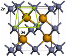
Figure 1. Crystal Structure of ZnSe in the Sphalerite Phase.
Zinc selenide (ZnSe) generally crystallizes in two main phases: the zinc blende (sphalerite) structure and the wurtzite structure. Under standard deposition conditions, the sphalerite cubic phase is dominant. It consists of a face-centered cubic (FCC) lattice where each selenium atom is tetrahedrally coordinated to four zinc atoms, and reciprocally. This tetrahedral geometry is illustrated in
Figure 1, which shows the zinc blende crystal structure of ZnSe
| [21] | Ikhioya, I. L., et al. Influence of precursor pH on Bi-doped ZnSe synthesized electrochemically. Applied Surface Science Advances. 2022, 9, 100232.
https://doi.org/10.1016/j.apsadv.2022.100232 |
| [22] | Lamonova, K. V., et al. ZnSe:(Cr, Fe) laser crystal matrices. Optical Materials: X. 2024, 22, 100321.
https://doi.org/10.1016/j.omx.2024.100321 |
| [23] | Chaparro, A. M., Maffiotte, C., Gutiérrez, M. T., Herrero, J. Morphological study of CBD-ZnSe thin films. Thin Solid Films. 2000, 358(1), 22-29.
https://doi.org/10.1016/S0040-6090(99)00704-X |
[21-23]
.
ZnSe thin films can be grown using several techniques, including chemical bath deposition (CBD), electrochemical routes, Bridgman crystal growth, and sputtering. Their crystalline quality, phase purity, microstructure, and possible strain effects are commonly assessed using X-ray diffraction (XRD) analysis
| [21] | Ikhioya, I. L., et al. Influence of precursor pH on Bi-doped ZnSe synthesized electrochemically. Applied Surface Science Advances. 2022, 9, 100232.
https://doi.org/10.1016/j.apsadv.2022.100232 |
| [22] | Lamonova, K. V., et al. ZnSe:(Cr, Fe) laser crystal matrices. Optical Materials: X. 2024, 22, 100321.
https://doi.org/10.1016/j.omx.2024.100321 |
| [23] | Chaparro, A. M., Maffiotte, C., Gutiérrez, M. T., Herrero, J. Morphological study of CBD-ZnSe thin films. Thin Solid Films. 2000, 358(1), 22-29.
https://doi.org/10.1016/S0040-6090(99)00704-X |
[21-23]
. Recent studies have highlighted the role of precursor chemistry, pH, annealing temperature, and dopant incorporation on grain size, dislocation density, and structural stability
| [7] | Mamo, S. G. Tailoring nonlinear plasmonic response of ZnSe@Ag and ZnSe@Au core-shell nanocomposites. Hybrid Advances. 2025, 11, 100562. https://doi.org/10.1016/j.hybadv.2025.100562 |
| [17] | Labadi, A., Tobbeche, S., Saidani, O., Bouladame, M., Brahimi, F. Efficiency improvement of CIGS solar cells with ZnSe buffer layer and SnS BSF layer. Micro and Nanostructures. 2025, 206, 208257.
https://doi.org/10.1016/j.micrna.2025.208257 |
| [24] | Somathube, S., et al. Synthesis of ZnSe QDs: optical and structural properties. Results in Physics. 2025, 73, 108262.
https://doi.org/10.1016/j.rinp.2025.108262 |
[7, 17, 24]
.
2.1.2. Optical Properties
ZnSe is a wide-bandgap II-VI semiconductor characterized by high optical transparency in the visible spectral range. In this work, the optical bandgap of ZnSe is not extracted experimentally but is taken as an input material parameter in the TCAD simulations. A bandgap value of Eg = 2.7 eV is adopted, consistent with widely reported experimental and theoretical studies
.
The large bandgap of ZnSe minimizes parasitic absorption in the buffer layer and enables favorable band alignment with the p-type CIGS absorber, contributing to reduced interface recombination and improved carrier selectivity
| [17] | Labadi, A., Tobbeche, S., Saidani, O., Bouladame, M., Brahimi, F. Efficiency improvement of CIGS solar cells with ZnSe buffer layer and SnS BSF layer. Micro and Nanostructures. 2025, 206, 208257.
https://doi.org/10.1016/j.micrna.2025.208257 |
| [18] | Soudagar, M. E. M., et al. Effect of electron transport layer thickness in hybrid CIGS cells. Journal of Power Sources. 2025, 639, 236657.
https://doi.org/10.1016/j.jpowsour.2025.236657 |
| [19] | Hossain, T., et al. Tuning the bandgap of Cd₁₋ₓZnₓS buffer layers for CIGS absorbers. Superlattices and Microstructures. 2022, 161, 107100.
https://doi.org/10.1016/j.spmi.2021.107100 |
[17-19]
.
2.1.3. Electrical Properties
Pristine ZnSe behaves as an intrinsic semiconductor, but its conductivity can be tuned to n-type or p-type depending on the dopant species. n-type ZnSe is obtained more easily through incorporation of halogen donors such as Cl, Br, or F, which introduce shallow donor levels. Achieving p-type ZnSe remains challenging due to the low solubility of acceptor dopants such as N or Cr
| [8] | Alghamdi, S. M. High-Efficiency BaZrSe3/ZnSe heterojunction solar cells: A numerical simulation approach. Results in Engineering. 2025, 28, 107195.
https://doi.org/10.1016/j.rineng.2025.107195 |
| [9] | Yoneta, M., Nanami, K., Uechi, H., Ohishi, M., Saito, H., Yoshino, K. Epitaxial growth and characterization of Cl-doped ZnSe layer by MBE. Journal of Crystal Growth. 2002, 237-239, 1545-1549. https://doi.org/10.1016/S0022-0248(01)02365-X |
| [20] | Talbi, A., et al. Co-doped ZnS buffer layers for high-efficiency solar cells. Chemical Physics Impact. 2025, 11, 100942.
https://doi.org/10.1016/j.chphi.2025.100942 |
[8, 9, 20]
.
The electrical conductivity and resistivity can be measured using the two-probe method, and are expressed as:
where
: is the measured current (A),
: the film thickness (cm),
: the cross-sectional area (cm²),
: the applied voltage (V),
: the resistivity at 0 K,
: the activation energy (eV),
: the Boltzmann constant,
the temperature (K).
Reported electron mobilities in high-quality ZnSe thin films often reach 100 cm²·V
-1·s
-1, while hole transport remains significantly lower, as commonly observed in II-VI semiconductors
| [8] | Alghamdi, S. M. High-Efficiency BaZrSe3/ZnSe heterojunction solar cells: A numerical simulation approach. Results in Engineering. 2025, 28, 107195.
https://doi.org/10.1016/j.rineng.2025.107195 |
| [9] | Yoneta, M., Nanami, K., Uechi, H., Ohishi, M., Saito, H., Yoshino, K. Epitaxial growth and characterization of Cl-doped ZnSe layer by MBE. Journal of Crystal Growth. 2002, 237-239, 1545-1549. https://doi.org/10.1016/S0022-0248(01)02365-X |
| [20] | Talbi, A., et al. Co-doped ZnS buffer layers for high-efficiency solar cells. Chemical Physics Impact. 2025, 11, 100942.
https://doi.org/10.1016/j.chphi.2025.100942 |
[8, 9, 20]
.
2.2. Electrical Model of the CIGS Solar Cell
2.2.1. Two-diode Equivalent Circuit
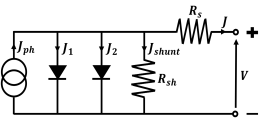
The CIGS solar cell operates as a classical p-n heterojunction, in which the p-type CIGS absorber and the n-type ZnSe buffer layer form the main junction. A two-diode equivalent model is employed to describe its electrical behavior, incorporating both bulk and interfacial recombination mechanisms.
Figure 2 presents the equivalent electrical circuit used in this study
| [10] | He, S., Zhang, Y., Yao, H., Zuo, H., Wang, H., Feng, G. Effect of impurity distribution on optical properties of Cr-doped ZnSe nanowires. Results in Physics. 2023, 48, 106459.
https://doi.org/10.1016/j.rinp.2023.106459 |
| [11] | Usama, M., et al. Optimizing ZnSe nanorods with La doping for device applications. Surfaces and Interfaces. 2024, 54, 105275. https://doi.org/10.1016/j.surfin.2024.105275 |
[10, 11]
.
Figure 2. Two-Diode Equivalent Electrical Model of a CIGS Solar Cell.
Under illumination, the terminal current density is expressed as:
(3)
where
is the photogenerated current density,
, the saturation current densities,
, the series and shunt resistances,
, the diode ideality factors,
the elementary charge,
the applied voltage,
the Boltzmann constant,
the temperature.
2.2.2. Fundamental Photovoltaic Parameters
Short-Circuit Current Density
where
1) : wavelength corresponding to the bandgap energy (m),
2) : incident spectral irradiance (W·m-2·nm-1),
3) : Planck constant (J·s),
4) : speed of light in vacuum (m·s-1),
5) : external quantum efficiency (dimensionless),
6) and
in the ideal case
.
Open-Circuit Voltage
where
1) : open-circuit voltage (V),
2) : diode ideality factor (1-2),
3) : Boltzmann constant (J·K-1),
4) : absolute temperature (K),
5) : reverse saturation current density (A·cm-2),
6)
: short-circuit current density (A·cm
-2)
| [13] | Vaas, T. S., et al. Light induced degradation of CIGS solar cells. Solar Energy Materials and Solar Cells. 2024, 275, 113036.
https://doi.org/10.1016/j.solmat.2024.113036 |
| [14] | Sikder, S., Hasan, M. K., Mamur, H., Bhuiyan, M. R. A. Enhancing CIGS solar cell performance via computational simulation. Hybrid Advances. 2025, 10, 100460.
https://doi.org/10.1016/j.hybadv.2025.100460 |
[13, 14]
.
Fill Factor (FF)
where
1) : fill factor (dimensionless),
2) : current density at maximum power point (A·cm-2),
3) : voltage at maximum power point (V),
4)
,
: as previously defined
| [13] | Vaas, T. S., et al. Light induced degradation of CIGS solar cells. Solar Energy Materials and Solar Cells. 2024, 275, 113036.
https://doi.org/10.1016/j.solmat.2024.113036 |
| [14] | Sikder, S., Hasan, M. K., Mamur, H., Bhuiyan, M. R. A. Enhancing CIGS solar cell performance via computational simulation. Hybrid Advances. 2025, 10, 100460.
https://doi.org/10.1016/j.hybadv.2025.100460 |
[13, 14]
.
Power Conversion Efficiency (η)
(7)
1) : power conversion efficiency (%),
2) : maximum output power density (W·cm-2),
3) : incident power density (W·cm-2),
4)
,
,
: as defined above
| [13] | Vaas, T. S., et al. Light induced degradation of CIGS solar cells. Solar Energy Materials and Solar Cells. 2024, 275, 113036.
https://doi.org/10.1016/j.solmat.2024.113036 |
| [14] | Sikder, S., Hasan, M. K., Mamur, H., Bhuiyan, M. R. A. Enhancing CIGS solar cell performance via computational simulation. Hybrid Advances. 2025, 10, 100460.
https://doi.org/10.1016/j.hybadv.2025.100460 |
[13, 14]
.
2.3. Numerical Simulation Framework
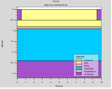
2.3.1. Device Structure
The simulated solar cell adopts the standard substrate configuration:
SLG / Mo / CIGS / ZnSe / ZnO / Al
The full device architecture is illustrated in
Figure 3, following
| [15] | Sharma, R., Himanshu, Patel, S. L., Chander, S., Kannan, M. D., Dhaka, M. S. Physical properties of ZnSe thin films. Physics Letters A. 2020, 384(4), 126097.
https://doi.org/10.1016/j.physleta.2019.126097 |
| [16] | Alam, F. E., Ali, B., Arif, S. Electric field and strain mediated ZnSe. Materials Advances. 2024.
https://doi.org/10.1039/D4MA00885E |
[15, 16]
.
Figure 3. Schematic Diagram of the Simulated CIGS/ZnSe/ZnO Solar Cell Structure.
2.3.2. Physical Models and Simulation Approach
Simulations were performed using the ATLAS-SILVACO device simulator. The following physical models were activated:
1) Poisson and drift-diffusion transport equations
2) Shockley-Read-Hall (SRH) recombination
3) Auger recombination
4) Wavelength-dependent optical generation (AM1.5G spectrum)
5) Thermionic emission at heterojunctions
6) Gaussian trap distributions in all layers
7) Fermi-Dirac carrier statistics
All simulations were conducted at:
1) Temperature: 300 K
2) Illumination: AM1.5G (1000 W·m-2)
3) Bias sweep: 0-1.5 V
Two parametric sweeps were performed:
1) ZnSe thickness: 0.02-0.10 µm
2) ZnSe donor concentration : 8×10¹⁶ - 1×1017 cm-3
2.3.3. Material Parameters Used in the Simulation
The material properties employed in ATLAS are summarized in
Table 1, directly inserted below for clarity and ease of reference.
Table 1. Material Properties Used for the CIGS/ZnSe/ZnO Solar Cell Model.
Parameter | CIGS | ZnO | ZnSe |
Bandgap Eg (eV) | 1.32 | 3.30 | 2.70 |
Thickness (µm) | 1.50 | 0.80 | 0.02-0.10 |
Electron affinity χ (eV) | 4.80 | 4.10 | 4.10 |
Relative permittivity εr | 13.6 | 9 | 10 |
NC (cm-3) | 2.2×10¹⁸ | 2.2×10¹⁸ | 2.2×10¹⁸ |
NV (cm-3) | 1.8×10¹⁹ | 1.8×10¹⁹ | 1.8×10¹⁹ |
Electron mobility μn (cm²·V-1·s-1) | 100 | 100 | 100 |
Hole mobility μp (cm²·V-1·s-1) | 25 | 25 | 25 |
Electron lifetime τn (s) | 1×10⁻⁷ | 1×10⁻⁷ | 1×10⁻⁷ |
Hole lifetime τp (s) | 1×10⁻⁷ | 1×10⁻⁷ | 1×10⁻⁷ |
Acceptor doping NA (cm-3) | 6×10¹⁶ | — | — |
Donor doping ND (cm-3) | — | 1×10¹⁸ | 8×10¹⁶-1×10¹⁸ |
2.3.4. Defect Parameters Incorporated in ATLAS
The Gaussian trap distributions implemented in ATLAS for each layer are listed in
Table 2.
Table 2. Gaussian Defect Parameters Used in CIGS, ZnO, and ZnSe Layers.
Parameter | CIGS | ZnO | ZnSe |
Trap concentration NG (cm-3) | 1×10¹³ | 1×10¹¹ | 1×10¹¹ |
Gaussian width W (eV) | 0.10 | 0.10 | 0.10 |
Peak energy EG (eV) | 0.60 | 1.65 | 1.35 |
Electron capture cross-section σn (cm²) | 1×10-17 | 1×10-17 | 1×10-17 |
Hole capture cross-section σp (cm²) | 1×10-15 | 1×10-15 | 1×10-15 |
All material, transport, recombination, and defect parameters used in the ATLAS simulations were adopted from well-established TCAD studies on CIGS and Cd-free buffer layers
| [25] | Dabbabi, S., Nasr, T. B., Kamoun-Turki, N. Parameters optimization of CIGS solar cell using 2D physical modeling. Results in Physics. 2017, 7, 4020-4024.
https://doi.org/10.1016/j.rinp.2017.06.057 |
| [26] | Elbar, M., Tobbeche, S. Numerical simulation of CGS/CIGS single and tandem thin-film solar cells using the SILVACO-ATLAS software. Energy Procedia. 2015, 74, 1220-1227. https://doi.org/10.1016/j.egypro.2015.07.766 |
| [27] | Bouanani, B., Joti, A., Bachir Bouiadjra, F. S., Kadid, A. Band gap and thickness optimization for improvement of CIGS/CIGS tandem solar cells using SILVACO software. Optik. 2020, 204, 164217.
https://doi.org/10.1016/j.ijleo.2020.164217 |
| [28] | Bechlaghem, S., Zebentout, B., Benamara, Z. The major influence of the conduction-band-offset onZn(O, S)/CuIn0.7Ga0.3Se2 solar cells. Results in Physics. 2018, 10, 650-654. https://doi.org/10.1016/j.rinp.2018.07.006 |
[25-28]
. These values fall within commonly accepted ranges reported in the literature and ensure the physical consistency and reproducibility of the simulations.
3. Results and Discussion
3.1. Effect of ZnSe Buffer-layer Thickness
The influence of the ZnSe buffer-layer thickness on the electrical performance of the CIGS solar cell is analyzed through the
characteristics, the short-circuit current density
, the open-circuit voltage
, the fill factor (
), and the power conversion efficiency (
). The ZnSe thickness is varied between 0.02 and 0.10 µm, which covers the typical range investigated for alternative Cd-free buffer layers in CIGS solar cells
| [18] | Soudagar, M. E. M., et al. Effect of electron transport layer thickness in hybrid CIGS cells. Journal of Power Sources. 2025, 639, 236657.
https://doi.org/10.1016/j.jpowsour.2025.236657 |
| [19] | Hossain, T., et al. Tuning the bandgap of Cd₁₋ₓZnₓS buffer layers for CIGS absorbers. Superlattices and Microstructures. 2022, 161, 107100.
https://doi.org/10.1016/j.spmi.2021.107100 |
| [21] | Ikhioya, I. L., et al. Influence of precursor pH on Bi-doped ZnSe synthesized electrochemically. Applied Surface Science Advances. 2022, 9, 100232.
https://doi.org/10.1016/j.apsadv.2022.100232 |
[18, 19, 21]
.
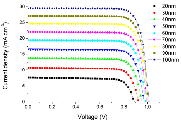
3.1.1. Influence of ZnSe Thickness on the J-V Characteristics
The evolution of the current-voltage characteristics for the different ZnSe thicknesses is presented in
Figure 4.
Figure 4. J-V characteristics Simulated for Various ZnSe Buffer-Layer Thicknesses.
As shown in
Figure 4, the J-V curves do not overlap; instead, they exhibit a strong dependence on the ZnSe thickness. The short-circuit current density (J
SC) increases from 7.66 mA·cm
-2 for a 0.02 µm ZnSe layer to about 29.56 mA·cm
-2 for 0.10 µm. Likewise, the open-circuit voltage (V
OC) rises from approximately 0.89 V to nearly 1.01 V as the thickness increases.
This behavior confirms that ZnSe thickness plays a critical role in controlling interface recombination and heterojunction quality. Very thin buffer layers generally induce strong interface defects and incomplete junction formation, leading to poor charge extraction. Conversely, moderately thicker layers improve electrostatic band alignment and suppress interfacial recombination, which enhances both J_SC and V
OC, as commonly reported in numerical and experimental CIGS studies
| [12] | Boukortt, N. E. I., Loureiro, A. G., Abushattal, A. Efficiency improvement of ultrathin CIGS solar cells. Solar Energy. 2024, 282, 112935. https://doi.org/10.1016/j.solener.2024.112935 |
| [13] | Vaas, T. S., et al. Light induced degradation of CIGS solar cells. Solar Energy Materials and Solar Cells. 2024, 275, 113036.
https://doi.org/10.1016/j.solmat.2024.113036 |
| [14] | Sikder, S., Hasan, M. K., Mamur, H., Bhuiyan, M. R. A. Enhancing CIGS solar cell performance via computational simulation. Hybrid Advances. 2025, 10, 100460.
https://doi.org/10.1016/j.hybadv.2025.100460 |
| [17] | Labadi, A., Tobbeche, S., Saidani, O., Bouladame, M., Brahimi, F. Efficiency improvement of CIGS solar cells with ZnSe buffer layer and SnS BSF layer. Micro and Nanostructures. 2025, 206, 208257.
https://doi.org/10.1016/j.micrna.2025.208257 |
[12-14, 17]
.
A detailed parameter-by-parameter analysis (JSC, VOC, FF, η) is presented in the following sections.
3.1.2. Effect of ZnSe Thickness on the Short-circuit Current Density (JSC)
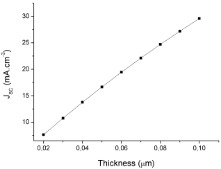
The variation of the short-circuit current density as a function of ZnSe thickness is shown in
Figure 5.
Figure 5. Evolution of the Short-Circuit Current Density as a Function of ZnSe Thickness.
Figure 5 shows a nearly linear increase in the short-circuit current density as the ZnSe thickness grows from 0.02 to 0.10 µm. Specifically, J
SC rises from 7.66 mA·cm
-2 at 0.02 µm to 29.56 mA·cm
-2 at 0.10 µm, indicating that thicker ZnSe layers systematically enhance carrier collection over the investigated range.
This behavior is consistent with a progressive improvement of the CIGS/ZnSe interface, leading to:
1) reduced interface recombination due to better surface coverage,
2) improved passivation as the buffer becomes more uniform,
3) a stronger built-in electric field favouring carrier extraction,
4) more favourable conduction-band alignment as the ZnSe layer approaches full continuity
| [12] | Boukortt, N. E. I., Loureiro, A. G., Abushattal, A. Efficiency improvement of ultrathin CIGS solar cells. Solar Energy. 2024, 282, 112935. https://doi.org/10.1016/j.solener.2024.112935 |
| [14] | Sikder, S., Hasan, M. K., Mamur, H., Bhuiyan, M. R. A. Enhancing CIGS solar cell performance via computational simulation. Hybrid Advances. 2025, 10, 100460.
https://doi.org/10.1016/j.hybadv.2025.100460 |
| [17] | Labadi, A., Tobbeche, S., Saidani, O., Bouladame, M., Brahimi, F. Efficiency improvement of CIGS solar cells with ZnSe buffer layer and SnS BSF layer. Micro and Nanostructures. 2025, 206, 208257.
https://doi.org/10.1016/j.micrna.2025.208257 |
[12, 14, 17]
.
It is important to note that the simulations could not be extended beyond 0.10 µm due to numerical convergence limitations in ATLAS. Work is currently underway to lift this constraint and explore whether an even thicker ZnSe layer could further enhance device performance. However, as will be discussed in the next subsection, the incipient saturation of the open-circuit voltage VOC suggests that the optimal thickness is likely very close to this value.
The detailed justification for this trend is presented in the following paragraph.
3.1.3. Effect of ZnSe Thickness on the Open-circuit Voltage (VOC)
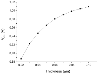
The variation of the open-circuit voltage as a function of ZnSe thickness is illustrated in
Figure 6.
Figure 6. Variation of the Open-Circuit Voltage as a Function of ZnSe Buffer-Layer Thickness.
Figure 6 shows that V
OC increases nearly linearly as the ZnSe thickness grows from 0.02 to 0.10 µm, rising from 0.887 V to approximately 1.009 V.
This evolution indicates that thicker ZnSe layers contribute to improved junction quality and reduced recombination at the CIGS/ZnSe interface.
The observed increase in VOC can be attributed to:
1) a progressive reduction in interface trap density as the buffer becomes more continuous,
2) a decrease in the dark saturation current density J0,
3) improved band alignment reducing thermionic recombination losses,
4) enhanced passivation effects that suppress Shockley-Read-Hall recombination in the depletion region
| [12] | Boukortt, N. E. I., Loureiro, A. G., Abushattal, A. Efficiency improvement of ultrathin CIGS solar cells. Solar Energy. 2024, 282, 112935. https://doi.org/10.1016/j.solener.2024.112935 |
| [14] | Sikder, S., Hasan, M. K., Mamur, H., Bhuiyan, M. R. A. Enhancing CIGS solar cell performance via computational simulation. Hybrid Advances. 2025, 10, 100460.
https://doi.org/10.1016/j.hybadv.2025.100460 |
| [17] | Labadi, A., Tobbeche, S., Saidani, O., Bouladame, M., Brahimi, F. Efficiency improvement of CIGS solar cells with ZnSe buffer layer and SnS BSF layer. Micro and Nanostructures. 2025, 206, 208257.
https://doi.org/10.1016/j.micrna.2025.208257 |
[12, 14, 17]
.
Unlike the previously reported non-monotonic behavior, the updated simulation results reveal a smooth and quasi-linear rise in VOC, with no degradation within the explored range.
However, the gradual flattening of the curve as the thickness approaches 0.10 µm indicates the onset of voltage saturation, suggesting that further increases in ZnSe thickness might provide only marginal improvements. This behaviour is commonly reported in optimized CIGS heterojunctions where increasing buffer-layer thickness eventually yields diminishing returns due to band-offset stabilization and saturation of interface passivation effects
| [12] | Boukortt, N. E. I., Loureiro, A. G., Abushattal, A. Efficiency improvement of ultrathin CIGS solar cells. Solar Energy. 2024, 282, 112935. https://doi.org/10.1016/j.solener.2024.112935 |
| [19] | Hossain, T., et al. Tuning the bandgap of Cd₁₋ₓZnₓS buffer layers for CIGS absorbers. Superlattices and Microstructures. 2022, 161, 107100.
https://doi.org/10.1016/j.spmi.2021.107100 |
[12, 19]
.
It is worth noting that the simulation could not be extended beyond 0.10 µm because of numerical convergence limitations in ATLAS. We are currently working on adjusting the meshing, boundary conditions, and defect modelling to remove this constraint and identify the true optimal thickness.
Nevertheless, the emerging saturation trend strongly suggests that this optimum is likely very close to 0.10 µm.
3.1.4. Effect of ZnSe Thickness on the Fill Factor (FF)
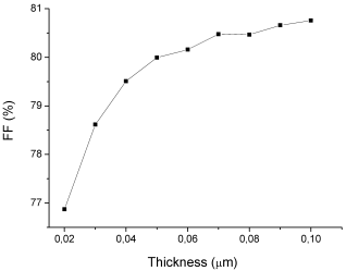
The variation of the fill factor according to ZnSe thickness is shown in
Figure 7.
Figure 7. Evolution of the Fill Factor as a Function of ZnSe Buffer-Layer Thickness.
Figure 7 shows that the fill factor increases steadily as the ZnSe thickness is varied from 0.02 to 0.10 µm, rising from approximately 78.84% to 81.01%.
The improvement is most pronounced in the thinner-layer region (0.02-0.06 µm), where the FF responds sensitively to the reduction of interface defects and the progressive homogenization of the ZnSe coverage.
Beyond 0.07 µm, the increase becomes more gradual, revealing a beginning of saturation. This behavior likely arises from:
1) enhanced passivation of interface states,
2) improved conduction-band alignment that stabilizes the junction’s transport properties,
3) reduced series resistance as the buffer thickness becomes sufficient to ensure uniform charge transfer,
4) suppression of localized recombination pathways due to better crystalline continuity
| [12] | Boukortt, N. E. I., Loureiro, A. G., Abushattal, A. Efficiency improvement of ultrathin CIGS solar cells. Solar Energy. 2024, 282, 112935. https://doi.org/10.1016/j.solener.2024.112935 |
| [14] | Sikder, S., Hasan, M. K., Mamur, H., Bhuiyan, M. R. A. Enhancing CIGS solar cell performance via computational simulation. Hybrid Advances. 2025, 10, 100460.
https://doi.org/10.1016/j.hybadv.2025.100460 |
| [17] | Labadi, A., Tobbeche, S., Saidani, O., Bouladame, M., Brahimi, F. Efficiency improvement of CIGS solar cells with ZnSe buffer layer and SnS BSF layer. Micro and Nanostructures. 2025, 206, 208257.
https://doi.org/10.1016/j.micrna.2025.208257 |
[12, 14, 17]
.
The saturation trend observed near 0.10 µm suggests that the FF is approaching its optimum in this region. Additional simulations beyond this thickness, currently limited by convergence, would help determine whether the maximum FF lies just above the explored range or is already reached.
Taken together with the trends in JSC and VOC, these results confirm that ZnSe thicknesses close to 0.10 µm provide the best overall device performance.
3.1.5. Effect of ZnSe Thickness on Power Conversion Efficiency (η)
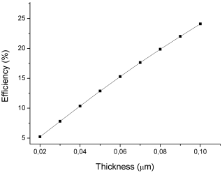
The evolution of the power conversion efficiency as a function of ZnSe thickness is shown in
Figure 8.
Figure 8. Evolution of the Power Conversion Efficiency η as a Function of ZnSe Buffer-Layer Thickness.
The efficiency increases steadily as the ZnSe thickness grows from 0.02 to 0.10 µm, rising from approximately 5.22% to 24.10%. This continuous improvement reflects the progressive enhancement of the short-circuit current density, the open-circuit voltage, and the fill factor as the buffer layer becomes thick enough to ensure proper heterojunction formation and stable carrier transport.
For very thin layers (0.02-0.05 µm), the low efficiency arises from:
1) incomplete surface coverage,
2) significant interface recombination due to insufficient passivation,
3) a weak electric field at the CIGS/ZnSe interface that limits charge separation.
As the ZnSe thickness increases, these limitations diminish. Improved structural homogeneity, better band alignment, and reduced trap-assisted recombination lead to stronger carrier collection and higher photovoltaic performance.
A noticeable reduction in the slope of η is observed near 0.10 µm, which suggests the beginning of a saturation regime. This indicates that the device may be approaching its optimal ZnSe thickness. Further simulations beyond 0.10 µm, once convergence constraints are resolved, will be required to accurately identify the true maximum.
Such trends are consistent with reported behaviors in CIGS devices using wide-bandgap buffer layers, where intermediate thicknesses achieve the best compromise between passivation quality and carrier transport
| [17] | Labadi, A., Tobbeche, S., Saidani, O., Bouladame, M., Brahimi, F. Efficiency improvement of CIGS solar cells with ZnSe buffer layer and SnS BSF layer. Micro and Nanostructures. 2025, 206, 208257.
https://doi.org/10.1016/j.micrna.2025.208257 |
| [19] | Hossain, T., et al. Tuning the bandgap of Cd₁₋ₓZnₓS buffer layers for CIGS absorbers. Superlattices and Microstructures. 2022, 161, 107100.
https://doi.org/10.1016/j.spmi.2021.107100 |
| [20] | Talbi, A., et al. Co-doped ZnS buffer layers for high-efficiency solar cells. Chemical Physics Impact. 2025, 11, 100942.
https://doi.org/10.1016/j.chphi.2025.100942 |
[17, 19, 20]
.
3.1.6. Intermediate Conclusion
The combined analysis of the J-V characteristics, the short-circuit current density JSC, the open-circuit voltage VOC, the fill factor (FF), and the conversion efficiency (η) confirms that the ZnSe buffer-layer thickness plays a decisive role in determining the performance of the CIGS solar cell.
Across the entire investigated range (0.02-0.10 µm), all photovoltaic parameters improve steadily, reflecting a progressive enhancement of interface quality and carrier-collection efficiency:
1. Very thin layers (< 0.06 µm) lead to incomplete junction formation, poor surface passivation, and elevated interface recombination, which significantly reduces JSC, VOC, FF, and η.
Such behavior is typical for wide-bandgap buffer layers when they are too thin to ensure proper coverage and defect suppression
| [15] | Sharma, R., Himanshu, Patel, S. L., Chander, S., Kannan, M. D., Dhaka, M. S. Physical properties of ZnSe thin films. Physics Letters A. 2020, 384(4), 126097.
https://doi.org/10.1016/j.physleta.2019.126097 |
| [17] | Labadi, A., Tobbeche, S., Saidani, O., Bouladame, M., Brahimi, F. Efficiency improvement of CIGS solar cells with ZnSe buffer layer and SnS BSF layer. Micro and Nanostructures. 2025, 206, 208257.
https://doi.org/10.1016/j.micrna.2025.208257 |
| [21] | Ikhioya, I. L., et al. Influence of precursor pH on Bi-doped ZnSe synthesized electrochemically. Applied Surface Science Advances. 2022, 9, 100232.
https://doi.org/10.1016/j.apsadv.2022.100232 |
[15, 17, 21]
.
2. As the ZnSe thickness increases, junction quality improves, and recombination losses decrease.
This results in monotonic increases of J
SC, V
OC, and FF, consistent with reported trends for optimized Cd-free CIGS interfaces
| [17] | Labadi, A., Tobbeche, S., Saidani, O., Bouladame, M., Brahimi, F. Efficiency improvement of CIGS solar cells with ZnSe buffer layer and SnS BSF layer. Micro and Nanostructures. 2025, 206, 208257.
https://doi.org/10.1016/j.micrna.2025.208257 |
| [20] | Talbi, A., et al. Co-doped ZnS buffer layers for high-efficiency solar cells. Chemical Physics Impact. 2025, 11, 100942.
https://doi.org/10.1016/j.chphi.2025.100942 |
[17, 20]
.
3. At 0.10 µm, the device reaches its highest simulated performance, with η exceeding 24%.
The slight slowing of improvement near 0.10 µm suggests that the optimal thickness lies close to this value, as expected when the buffer layer becomes sufficiently thick to stabilize the electric field while avoiding excessive absorption or transport resistance
.
It should be noted that simulations above 0.10 µm were not completed due to numerical convergence limitations. Work is currently underway to extend the analysis and confirm the exact optimum. However, the incipient performance saturation observed in VOC and FF strongly suggests that the true optimum is located only slightly above 0.10 µm.
Overall, the results validate that the near-optimal ZnSe thickness range is around 0.10 µm, in close agreement with trends previously reported for high-performance Cd-free CIGS device architectures
| [17] | Labadi, A., Tobbeche, S., Saidani, O., Bouladame, M., Brahimi, F. Efficiency improvement of CIGS solar cells with ZnSe buffer layer and SnS BSF layer. Micro and Nanostructures. 2025, 206, 208257.
https://doi.org/10.1016/j.micrna.2025.208257 |
| [20] | Talbi, A., et al. Co-doped ZnS buffer layers for high-efficiency solar cells. Chemical Physics Impact. 2025, 11, 100942.
https://doi.org/10.1016/j.chphi.2025.100942 |
| [21] | Ikhioya, I. L., et al. Influence of precursor pH on Bi-doped ZnSe synthesized electrochemically. Applied Surface Science Advances. 2022, 9, 100232.
https://doi.org/10.1016/j.apsadv.2022.100232 |
[17, 20, 21]
.
3.2. Effect of ZnSe Buffer Layer Doping Concentration
The influence of the ZnSe buffer-layer doping concentration on the performance of the CIGS solar cell is evaluated through the J-V characteristics, the short-circuit current density JSC, the open-circuit voltage VOC, and the main photovoltaic parameters.
In this study, the doping concentration is varied over a wide interval, from 8×10
16 cm
−3 to 1×10
18 cm
−3, allowing a detailed assessment of how increasing donor density affects carrier transport, recombination, and band alignment in the CIGS/ZnSe heterojunction. Such doping levels are commonly used in the optimization of wide-band-gap Cd-free buffer layers and are consistent with previously reported design guidelines for ZnSe- and ZnS-based architectures
| [17] | Labadi, A., Tobbeche, S., Saidani, O., Bouladame, M., Brahimi, F. Efficiency improvement of CIGS solar cells with ZnSe buffer layer and SnS BSF layer. Micro and Nanostructures. 2025, 206, 208257.
https://doi.org/10.1016/j.micrna.2025.208257 |
| [20] | Talbi, A., et al. Co-doped ZnS buffer layers for high-efficiency solar cells. Chemical Physics Impact. 2025, 11, 100942.
https://doi.org/10.1016/j.chphi.2025.100942 |
| [29] | Pandey, K., et al. Suitable buffer layers for PbS quantum dot solar cells using SCAPS-1D. Optik. 2024, 298, 171593.
https://doi.org/10.1016/j.ijleo.2023.171593 |
[17, 20, 29]
.
This analysis provides a basis for identifying the optimal doping range that maximizes JSC, enhances VOC, and ensures a balanced compromise between reduced series resistance and controlled interface recombination.
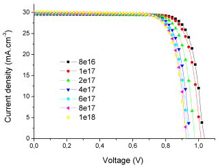
3.2.1. Influence of ZnSe Doping on the J-V Characteristics
The evolution of the current-voltage characteristics for different ZnSe doping concentrations is shown in
Figure 9.
Figure 9. Simulated J-V Characteristics for Various ZnSe Buffer Layer Doping Concentrations.
The simulated J-V curves exhibit clear variations as the ZnSe donor concentration increases from 8×10¹⁶ to 1×1018 cm−3. Two main trends emerge:
1) Increase in short-circuit current density JSC
As the doping level increases, the curves shift upward, with JSC increasing from 29.56 mA·cm-2 at 8×1016 cm−3 to 30.22 mA·cm-2 at 1×1018 cm−3.
This enhancement can be attributed to:
a) a stronger electric field at the ZnSe/CIGS interface,
b) a reduction in interfacial barrier height for electron extraction,
c) a decrease in recombination losses within the buffer region for moderately high doping
| [17] | Labadi, A., Tobbeche, S., Saidani, O., Bouladame, M., Brahimi, F. Efficiency improvement of CIGS solar cells with ZnSe buffer layer and SnS BSF layer. Micro and Nanostructures. 2025, 206, 208257.
https://doi.org/10.1016/j.micrna.2025.208257 |
| [20] | Talbi, A., et al. Co-doped ZnS buffer layers for high-efficiency solar cells. Chemical Physics Impact. 2025, 11, 100942.
https://doi.org/10.1016/j.chphi.2025.100942 |
[17, 20]
.
2) Decrease in open-circuit voltage VOC
At the same time, the open-circuit voltage gradually decreases from ≈1.026 V at low doping to ≈0.919 V at the highest level.
This decline is typically linked to:
a) an increase in the saturation current density J0,
b) enhanced recombination within the heavily doped ZnSe layer,
c) a slight deterioration of the conduction-band offset at the heterojunction interface
Interpretation
The combined behavior highlights a doping-induced trade-off:
d) Higher doping improves current collection,
e) but simultaneously reduces voltage stability.
A more detailed assessment of JSC, VOC, the fill factor, and the conversion efficiency is therefore necessary, as presented in the following subsections.
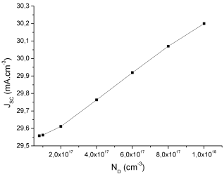
3.2.2. Effect of ZnSe Doping on the Short-circuit Current Density ()
The variation of the short-circuit current density
with respect to the ZnSe doping concentration is depicted in
Figure 10.
Figure 10. Variation of the Short-Circuit Current Density as a Function of ZnSe Doping Concentration.
According to
Figure 10, J
SC shows a slight but consistent increase as the ZnSe donor concentration rises from 8×10
16 to 1×10
18 cm
−3.
More specifically, the short-circuit current density increases from 29.56 mA·cm-2 at the lowest doping level to 30.22 mA·cm-2 at the highest concentration.
This gradual enhancement can be attributed to several mechanisms:
1) strengthening of the electric field at the ZnSe/CIGS interface, which improves charge separation and extraction,
2) reduction of the effective barrier height for electron transport as donor density increases,
3) suppression of interface recombination through improved band bending in the depletion region
| [17] | Labadi, A., Tobbeche, S., Saidani, O., Bouladame, M., Brahimi, F. Efficiency improvement of CIGS solar cells with ZnSe buffer layer and SnS BSF layer. Micro and Nanostructures. 2025, 206, 208257.
https://doi.org/10.1016/j.micrna.2025.208257 |
| [20] | Talbi, A., et al. Co-doped ZnS buffer layers for high-efficiency solar cells. Chemical Physics Impact. 2025, 11, 100942.
https://doi.org/10.1016/j.chphi.2025.100942 |
[17, 20]
.
These observations are consistent with reports showing that moderate-to-high doping levels in wide-bandgap buffer layers can enhance carrier collection without significantly modifying the optical absorption properties, as most photogeneration occurs in the CIGS absorber
.
Overall, the weak dependence of JSC on ZnSe doping confirms that:
1) the absorber remains the dominant contributor to photocurrent generation,
2) the buffer layer plays mainly an electrical role, shaping interfacial fields rather than contributing to light absorption, in agreement with previous Cd-free CIGS studies involving ZnS, Zn(O, S), and In
2S
3 .
Although some studies report a slight reduction of JSC at high doping, the present simulation shows a small increase, which can be attributed to the specific band bending and interface conditions reproduced in ATLAS.
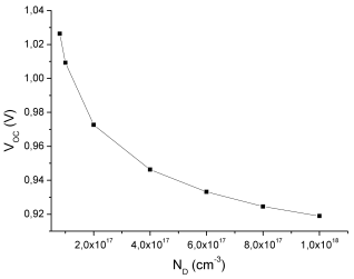
3.2.3. Effect of ZnSe Doping on the Open-circuit Voltage (VOC)
The variation of the open-circuit voltage
as a function of the ZnSe doping concentration is shown in
Figure 11.
Figure 11. Evolution of the Open-Circuit Voltage as a Function of ZnSe Buffer Layer Doping Concentration.
Figure 11 shows that V
OC decreases from 1.170 V to 1.054 V as the ZnSe doping concentration increases from 8×10
16 cm
-3 to 1×10
18 cm
-3.
Although the overall reduction remains moderate, the decline is more pronounced in the interval 8×10¹⁶-2×1017 cm-3, beyond which the decrease tends to slow down.
This behavior can be explained by:
1) an increase in the reverse saturation current density J0 when the doping becomes excessive,
2) a modification of the junction band bending that becomes less favorable for carrier separation,
3) an enhancement of non-radiative recombination within the depletion region as the electric field weakens at high dopant concentrations
| [17] | Labadi, A., Tobbeche, S., Saidani, O., Bouladame, M., Brahimi, F. Efficiency improvement of CIGS solar cells with ZnSe buffer layer and SnS BSF layer. Micro and Nanostructures. 2025, 206, 208257.
https://doi.org/10.1016/j.micrna.2025.208257 |
| [29] | Pandey, K., et al. Suitable buffer layers for PbS quantum dot solar cells using SCAPS-1D. Optik. 2024, 298, 171593.
https://doi.org/10.1016/j.ijleo.2023.171593 |
[17, 29]
.
Thus, as observed for JSC, the open-circuit voltage remains weakly sensitive to ZnSe doping as long as the concentration stays within a moderate range.
In the next section, the influence of doping on the fill factor, and more importantly on the overall power conversion efficiency, is examined to determine the doping interval that ensures the best device performance.
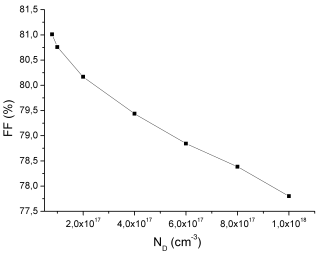
3.2.4. Effect of ZnSe Doping on the Fill Factor ()
The evolution of the fill factor as a function of the ZnSe buffer-layer doping concentration is presented in
Figure 12.
Figure 12. Evolution of the Fill Factor as a Function of the ZnSe Buffer-Layer Doping Level.
According to the updated dataset, the fill factor decreases continuously as the ZnSe doping concentration increases from 8×10¹⁶ to 1×1018 cm-3, dropping from 81.01% to 77.80%.
This monotonic decline indicates that increasing the donor concentration in the ZnSe buffer layer systematically deteriorates the diode quality.
Several physical mechanisms may explain this degradation:
1) increased ionized-impurity scattering, which reduces carrier mobility and increases resistive losses in the buffer region,
2) enhanced interface recombination due to dopant-induced defect formation near the CIGS/ZnSe heterojunction,
3) higher series resistance, a typical consequence of excessive doping in wide-bandgap buffer layers,
4) unfavorable modification of band bending, which limits efficient charge extraction.
Such behavior is consistent with previous observations in Cd-free buffer technologies: such as ZnS, Zn(O, S), and In
2S
3, where excessive doping systematically reduces FF due to increased recombination and resistive effects
.
Overall, these results show that higher ZnSe doping concentrations negatively impact the fill factor, and therefore contribute to the reduction of the total power conversion efficiency.
This makes the identification of a moderate doping range essential to balance interface quality and charge transport properties.
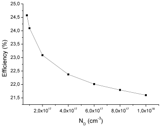
3.2.5. Effect of ZnSe Doping on the Power Conversion Efficiency (η)
The variation of the power conversion efficiency as a function of ZnSe doping concentration is shown in
Figure 13.
Figure 13. Evolution of the Power Conversion Efficiency as a Function of ZnSe Buffer-Layer Doping Level.
The results in
Figure 13 show that the efficiency decreases continuously as the ZnSe doping level increases from 8×10
16 to 1×10
18 cm
-3, falling from 24.58% to 21.60%.
Two distinct regions can nevertheless be identified based on the rate of degradation:
1) Rapid degradation at moderate doping levels (8×10¹⁶ - 2×1017 cm-3)
In this interval, η drops sharply from 24.58% to 23.09%.
This pronounced decline is primarily related to:
a) an increase in the reverse saturation current J0,
b) enhanced Shockley-Read-Hall recombination,
c) degradation of band alignment at the CIGS/ZnSe interface,
d) the formation of dopant-induced defect states within the buffer layer and at the heterojunction
.
These mechanisms reduce both VOC and FF, directly lowering efficiency.
2) Slower degradation at higher doping levels (2×10¹⁷ - 1×1018 cm-3)
Beyond 2×1017 cm-3, the efficiency continues to decrease, but at a reduced rate, from 23.09% to 21.60%.
This smoother decline suggests that excessive doping:
a) no longer contributes to band-structure improvement,
b) introduces additional recombination pathways,
c) reduces carrier mobility through ionized-impurity scattering,
d) perturbs the electrostatic potential distribution, limiting charge extraction.
Overall interpretation
Unlike thickness, where an optimum region emerges, ZnSe doping monotonically degrades the power conversion efficiency across the entire explored range.
This deterioration is strongly correlated with the corresponding decrease in the fill factor, which is itself highly sensitive to:
a) interfacial defect density,
b) resistive losses,
c) charge-transport limitations.
These results clearly indicate that high ZnSe doping levels are detrimental to CIGS performance, confirming that only moderate dopant concentrations should be considered for Cd-free buffer optimization.
3.2.6. Overall Conclusion on the Influence of ZnSe Thickness and Doping
A consolidated analysis of the photovoltaic parameters provides a coherent understanding of the impact of ZnSe buffer-layer engineering on the performance of CIGS solar cells.
Influence of ZnSe Thickness
Although ZnSe thickness has only a minor effect on the open-circuit voltage VOC, it significantly influences the other key photovoltaic parameters:
1) the short-circuit current density JSC,
2) the fill factor (FF),
3) the power conversion efficiency (η).
The updated simulations show that increasing ZnSe thickness progressively improves device performance, mainly due to:
1) better junction formation,
2) reduced interface recombination losses,
3) improved carrier-collection efficiency.
The optimal performance range corresponds to 0.08-0.10 µm, where efficiency approaches its maximum and begins to show early signs of saturation, suggesting proximity to the true optimal point.
The limiting value of 0.10 µm arises from numerical convergence constraints; future work will aim to extend the simulation domain to confirm the exact optimal thickness.
Influence of ZnSe Doping
The doping concentration of ZnSe exerts only a weak influence on JSC and VOC, but it has a strong and systematic impact on:
1) the fill factor,
2) the overall conversion efficiency.
Increasing the doping concentration leads to:
1) enhanced trap-assisted recombination,
2) stronger ionized-impurity scattering,
3) deterioration of band bending and electric-field distribution,
4) higher resistive losses.
These effects contribute to the monotonic degradation of FF and efficiency, confirming that ZnSe performs best under moderate doping conditions.
The optimal doping concentration is found to be: 8×10
16 - 2×10
17 cm
-3, in agreement with previous studies on Cd-free buffer layers in CIGS devices
| [18] | Soudagar, M. E. M., et al. Effect of electron transport layer thickness in hybrid CIGS cells. Journal of Power Sources. 2025, 639, 236657.
https://doi.org/10.1016/j.jpowsour.2025.236657 |
| [20] | Talbi, A., et al. Co-doped ZnS buffer layers for high-efficiency solar cells. Chemical Physics Impact. 2025, 11, 100942.
https://doi.org/10.1016/j.chphi.2025.100942 |
| [21] | Ikhioya, I. L., et al. Influence of precursor pH on Bi-doped ZnSe synthesized electrochemically. Applied Surface Science Advances. 2022, 9, 100232.
https://doi.org/10.1016/j.apsadv.2022.100232 |
[18, 20, 21]
.
Optimal Parameters for ZnSe as a Buffer Layer
By combining the separate influences of thickness and doping, the optimal ZnSe configuration for maximizing CIGS cell efficiency is:
1) ZnSe thickness: 0.08 - 0.10 µm
2) ZnSe doping concentration: 8×10¹⁶ - 2×1017 cm-3
This optimized design provides the best compromise between junction quality, carrier collection, interface passivation, and recombination suppression. These results align with current literature demonstrating that wide-bandgap, Cd-free buffer layers must be carefully engineered to achieve high-efficiency CIGS devices
| [18] | Soudagar, M. E. M., et al. Effect of electron transport layer thickness in hybrid CIGS cells. Journal of Power Sources. 2025, 639, 236657.
https://doi.org/10.1016/j.jpowsour.2025.236657 |
| [20] | Talbi, A., et al. Co-doped ZnS buffer layers for high-efficiency solar cells. Chemical Physics Impact. 2025, 11, 100942.
https://doi.org/10.1016/j.chphi.2025.100942 |
| [21] | Ikhioya, I. L., et al. Influence of precursor pH on Bi-doped ZnSe synthesized electrochemically. Applied Surface Science Advances. 2022, 9, 100232.
https://doi.org/10.1016/j.apsadv.2022.100232 |
[18, 20, 21]
.